|
Molecular Electronics
|
|
|
Self-assembled monolayers (SAMs) are promising
candidates as active components in molecular electronics. A major disadvantage
in organic molecule-based electronic devices is that the stability and
robustness of organic systems, in general, are less than their inorganic
counterparts. The development of nanoscale insulators and dielectrics,
molecular switches, rectifiers, and field effect transistors, require that
organic molecules have sufficient stability against electrical breakdowns. STM
provides a rapid and precise means to systematically survey the electronic
properties as well as the structure and stability of SAMs prior to device
fabrication. In addition to high-resolution structural characterization, STM
can be used to mimic the interfacial junctions in electronic devices, by
regulating tip-surface interactions. We have developed a new method, by
combining STM structural characterization with spectroscopy measurements, to
investigate the electronic properties of single organic molecules and
nanoparticles.
|
|
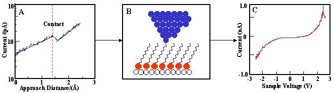
Scanning tunneling spectroscopy of decanethiol SAMs on Au(111). (A)
A typical current-distance curve of decanethiol SAMs measured from the setpoint
(I = 50 pA and V = 1.0 V). The contact between the tip and the monolayer
surface is defined as the first kink point on the lnI-Z curve, indicated by the
dash line. (B) STM tip is approached at contact with the methyl group of
decanethiols. (C) I-V characteristics of decanethiol SAMs when the tip is at
contact with the SAM surface. At 2.4 V (sample positive), a peak with negative
differential resistance is present.
|
|
|
|
|
|
|
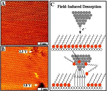
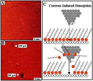 Current-induced
desorption by STM. Images of a decanethiol SAM were taken before (A) and after
(B) fabrication. A 1 nm hole was fabricated at +1.0 V and 200 pA, and a hole of
3 nm formed at 300 pA. (C) Schematic diagram of the desorption procedure using
tunneling electrons. Current-induced
desorption by STM. Images of a decanethiol SAM were taken before (A) and after
(B) fabrication. A 1 nm hole was fabricated at +1.0 V and 200 pA, and a hole of
3 nm formed at 300 pA. (C) Schematic diagram of the desorption procedure using
tunneling electrons.
|
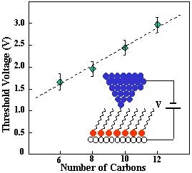
Breacdown threshold voltages as a
function of the number of carbons in the alkylthiol chains. Measurements were
conducted at the tip-SAM contact point. The straight line represents the least
square fit with a slope of 1.9 * 109 V/m.
|
|
| Publications:
(1). Yang, G.; Liu, G-Y. New insights for self-assembled monolayers for organothiols revealed by scanning tunneling microscopy (feature article), J. Phys. Chem. B 2003, 107, 8746-8759. (2). Yang, G.; Amro, N. A.; Liu, G-Y. Scanning probe lithography of self-assembled monolayers, Proc. SPIE 2003, 5220, 52-65. |
|