
|
|
|||||
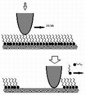
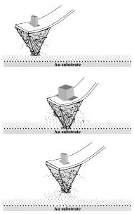
| 1. Nanoshaving | |||||
|

|
||||
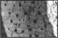
| Fig. 1 160 × 160 nm2 topographic image of C18S/Au(111) with the thiols shaved away from the central 50 × 50 nm2 square. | |||||
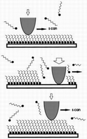
| 2. Nanografting | |||||
|
 |
 |
|||
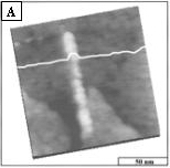
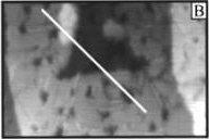
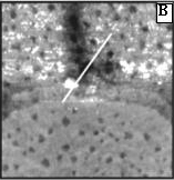
| Fig. 2 (A) A 200 × 200 nm2 topographic
image of a HOC2S/Au(111) matrix with a 75 × 100
nm2 C18S region. The C18SH
solution concentration was 0.2 mM, the displacement force was 20 nN, and the
scan rate was 50 ms/line. (B) Corresponding cursor profile showing the height
of the C18S region is 1.6 ± 0.2 nm taller than
the matrix. This value agrees with the expected thickness difference between
close-packed C18S and HOC2S SAMs.
|
|||||
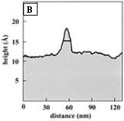
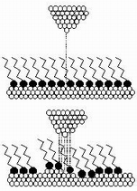
| 3. NanoPen Reader and Writer (NPRW) | |||||
 |
 |
 |
|||
| Fig. 3 nanopattern produced and imaged in
air within a C10S/Au SAM using NPRW: (A) a 10 × 100 nm2 line of CF12C2S
produced within the C10S/Au; (B) the corresponding cursor profile as indicated
in (A).
|
|||||
| 4. Electron induced diffusion | |||||
 |
 |
 |
|||
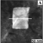
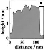
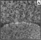
| Fig. 4 Example of tunneling electron-induced diffusion in C10S/Au(111). (A) A 75 × 50 nm2 constant-current STM topograph taken using a tungsten tip at 1.5 V and 6.6 pA. (B) After a triangular area was scanned at 80 pA. At this current, one layer of gold atoms under the SAM in the triangular area was displaced. | |||||
| 5. Electron induced evaporation | |||||
|
 |
 |
|||
| Fig. 5 Example of tunneling electron-induced evaporation of thiols in C10S/Au(111). (A) Constant-current STM topograph (100 × 100 nm2) acquired at a bias voltage of 2 V and tunneling current of 4 pA. (B) After an L-shaped area was scanned at 80 pA. | |||||
|
Publications:
(1) “Nanometer-Scale Fabrication by Simultaneous Nanoshaving and Molecular Self-Assembly” Xu, S.; Liu, G.-Y. Langmuir, 1997, 12, 127 - 129. (2) “Nanometer Scale Fabrication of Self-Assembled Monolayers: Nanoshaving and Nanografting” Liu, G.-Y.; Xu, S. In New Directions in Materials Synthesis, Ed. Winter, C. H.; Hoffman, D., 1998, ACS Symposium Series 727, 199. (3) “Fabrication of Nanometer Scale Patterns within Self-Assembled Monolayers by Nanografting” Xu, S.; Miller, S.; Laibinis, P. E.; Liu, G.-Y. Langmuir, 1999, 15, 7244-7251. (4) “Fabrication and Imaging of Nanometer-Sized Protein Patterns” Wadu-Mesthrige, K.; Xu, S.; Amro, N. A.; Liu, G.-Y.; Langmuir, 1999, 15, 8580-8583. (5) “Patterning Surfaces Using Tip Directed Displacement and Self-Assembly” Amro, N. A.; Xu, S.; Liu, G.-Y. Langmuir, 2000, 16(7), 3006-3009. (6) “Nanofabrication of Self-Assembled Monolayers Using Scanning Probe Lithography” Liu, G.-Y.; Xu, S.; Qian, Y. Acc. Chem. Res. 2000, 33, 457-466. (7) “Fabrication of Nanometer-Sized Protein Patterns Using Atomic Force Microscopy and Selective Immobilization” Wadu-Mesthrige, K.; Amro, N. A.; Garno, J. C.; Liu, G.-Y.; Biophysical J., 2001, 80, 1891-1899. (8) “Nanofabrication Using Computer-Assisted Design and Automated Vector-Scanning Probe Lithography” Cruchon-Dupeyrat, S.; Porthun, S.; Liu, G.-Y. Applied Surface Science, 2001, 175-176, 636-642. (9) “Characterization of AFM Tips Using Nanografting” Xu, S.; Amro, N.; Liu, G.-Y. Applied Surface Science, 2001, 175-176, 649-655. (10) ”Precise Positioning of Nanoparticles on Surfaces Using Scanning Probe Lithography” Garno, J. C.; Yang, Y.; Amro, N. A.; Cruchon-Dupeyrat, S.; Chen, S.; Liu, G. Y.; Nano Lett; 2003, 3(3): 389-395. |
|||||